Tungsten Targets for PVD Sputtering and Thin Film Deposition
-
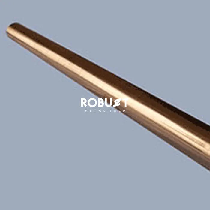
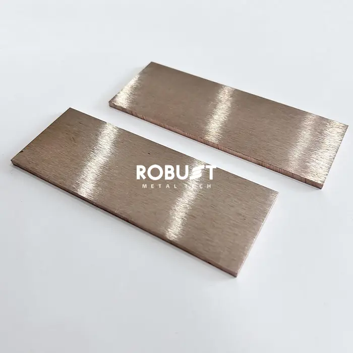
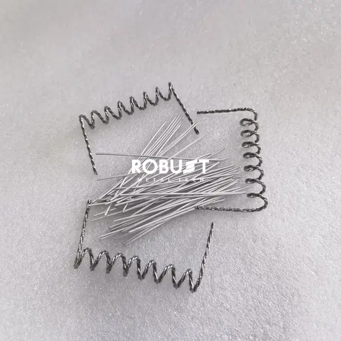
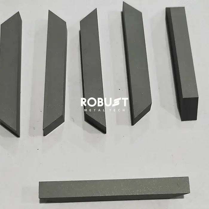
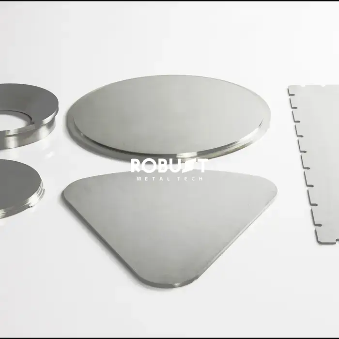
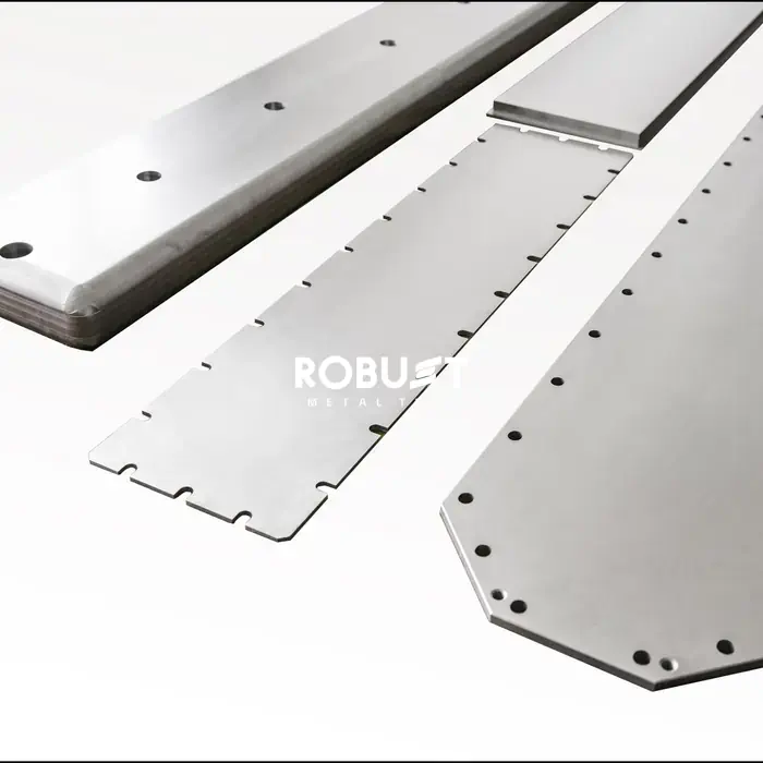
Tungsten targets are high-purity engineered materials used in PVD sputtering, thin-film deposition, and X-ray generation applications. They are produced as discs, blocks, or cylindrical forms with strict control over purity, density, and grain structure. These targets serve as sacrificial source materials in semiconductor manufacturing, medical imaging devices, and advanced coating systems. Available in pure tungsten and tungsten-based alloys such as W-Ti, WSi₂, WC, and W-Re, they deliver stable plasma performance and consistent film quality. High density and controlled microstructure ensure uniform erosion, reduced defects, and long service life in ultra-high vacuum environments critical to microelectronics and AI hardware production.
Description
Tungsten Targets
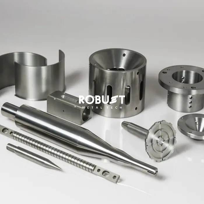
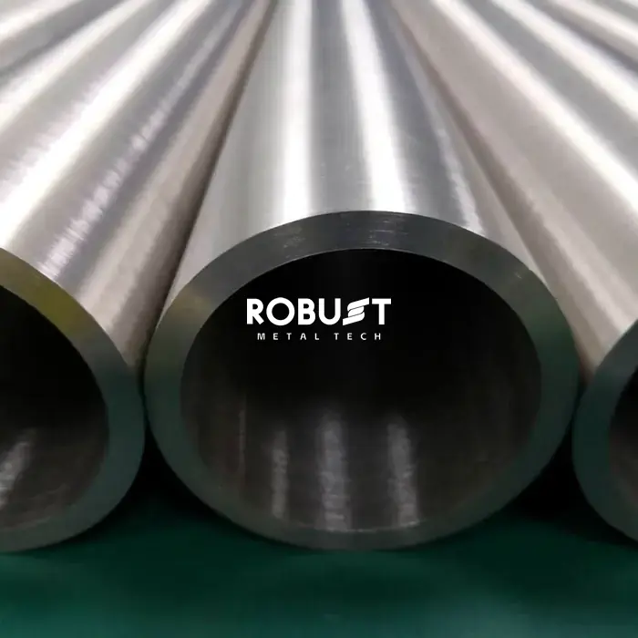
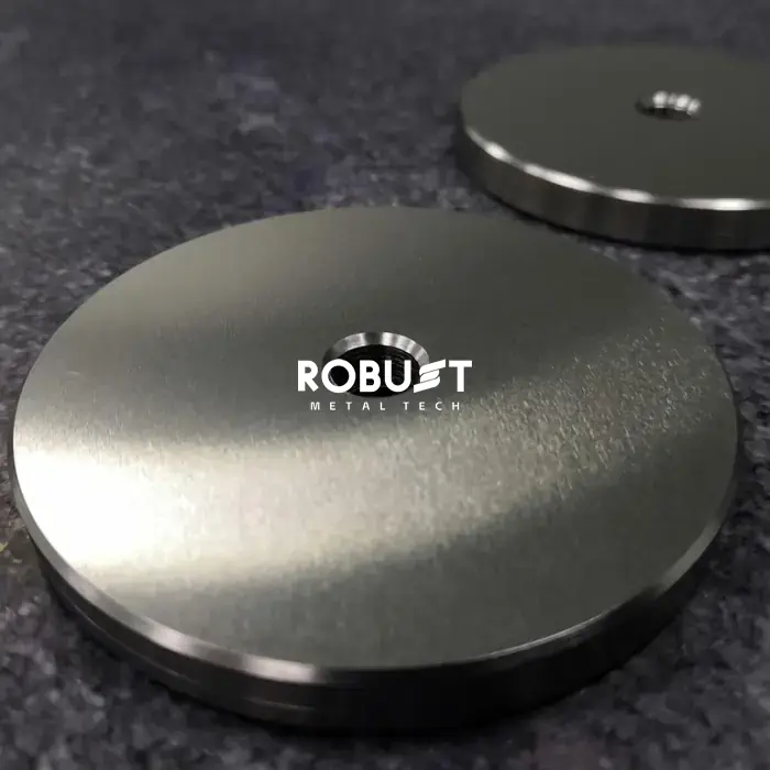
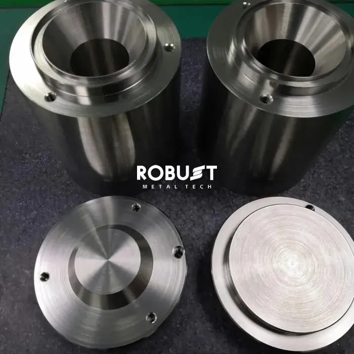
Tungsten targets are highly engineered blocks, discs, or cylinders of ultra-high-purity tungsten or tungsten alloys.
Unlike structural tungsten products, targets are sacrificial source materials used in advanced thin-film deposition technologies.
Main applications include Physical Vapor Deposition (PVD), sputtering systems, and X-ray generation.
They are critical materials in semiconductor, AI hardware, and medical imaging industries.
Application and Classification
Grades and Usage of Tungsten Targets
Pure Tungsten W1 (≥99.95%): Most common for thin film deposition.
Tungsten Alloys:
W-Ti (e.g., W-10%Ti): Diffusion barriers in semiconductor devices.
WSi₂ (Tungsten Silicide): Gate electrodes and interconnect layers.
WC (Tungsten-Carbon): Hard, wear-resistant coating applications.
W-Re (Tungsten-Rhenium): Improved ductility and thermal stability.
Doped Tungsten: Lanthanated (W-La) or rare-earth doped for electronic performance tuning.
Video
FAQs
FAQ – Tungsten Targets for PVD and X-Ray Applications
Q: Why is there a large price difference between 3N5 and 5N tungsten targets?
Higher purity requires advanced chemical refining to remove trace elements at ppb levels.
3N5–4N (99.95%–99.99%) is used for solar panels, displays, and decorative coatings.
5N–6N (99.999%–99.9999%) is required for semiconductor manufacturing.
Even trace impurities like alkali metals or radioactive elements can cause soft errors in silicon wafers.
Q: What is a W-Ti target and why is it used?
A tungsten-titanium target (commonly 90% W / 10% Ti) is widely used in semiconductor barrier layers.
Tungsten blocks diffusion between metal layers.
Titanium improves adhesion to silicon and copper or aluminum wiring layers.
Q: Why do grain size and texture matter in sputtering targets?
Plasma ion bombardment removes atoms based on crystal grain structure.
Fine and uniform grains (<100 μm) ensure even erosion and stable film thickness.
Large or irregular grains cause uneven erosion and reduce target lifetime.
Q: What is relative density and why is 99.5% important?
Relative density measures how close the material is to theoretical tungsten density (19.3 g/cm³).
Low density contains porosity, which causes gas release during sputtering.
This leads to “spitting” defects that contaminate substrates.
Q: Monolithic vs bonded tungsten targets?
Monolithic targets are single solid tungsten pieces, used in smaller or low-stress systems.
Bonded targets are attached to copper or aluminum backing plates using indium or diffusion bonding.
Backings improve cooling and reduce cracking from thermal stress.
Q: What is the temperature limit for indium-bonded targets?
Indium melts at 156.6°C.
If cooling fails or power is excessive, the bond layer can melt.
This causes separation between tungsten target and backing plate.
Q: What is utilization rate of tungsten targets?
Planar targets: 30%–40% utilization due to race-track erosion.
Rotary targets: 70%–80% utilization with more uniform wear.
Q: Can tungsten targets be recycled?
Yes. Spent targets still contain significant valuable tungsten material.
Recycling programs help reduce procurement cost and material waste.
Literature
Reliable Tungsten Targets for PVD Sputtering and Thin Film Deposition Manufacturer & Supplier in China
Robust provides high-quality Tungsten Targets for PVD Sputtering and Thin Film Deposition solutions for industrial, high-temperature, and precision engineering applications worldwide.
OEM & ODM Support | Fast Delivery | Factory Direct Price